- 您现在的位置:买卖IC网 > Sheet目录1228 > MAX367CWN (Maxim Integrated Products)IC SIGNAL-LINE CIRC PROT 18-SOIC
�� �
�
�Signal-Line� Circuit� Protectors�
�______________________________________________________________Pin� Description�
�PIN�
�NAME*�
�FUNCTION�
�MAX366�
�MAX367�
�1,� 2,� 3�
�–�
�4�
�–�
�5,� 6,� 7�
�8�
�1,� 2,� 3�
�4–8�
�9�
�10–14�
�15,� 16,� 17�
�18�
�IN1,� IN2,� IN3�
�IN4–IN8�
�V-�
�OUT8–OUT4�
�OUT3,� OUT2,�
�OUT1�
�V+�
�Signal� Inputs� 1,� 2,� 3�
�Signal� Inputs� 4–8�
�Negative� Supply� Voltage� Input�
�Signal� Outputs� 4–8�
�Signal� Outputs� 1,� 2,� 3�
�Positive� Supply� Voltage� Input�
�*� Inputs� and� outputs� are� names� for� convenience� only;� inputs� and� outputs� are� identical� and� interchangeable.�
�___________Background� Information�
�When� a� voltage� outside� the� supply� range� is� applied� to�
�most� integrated� circuits,� there� is� a� strong� possibility� they�
�will� be� damaged� or� “latch� up”� (that� is,� fail� to� operate� prop-�
�erly� even� after� the� offending� voltage� is� removed).� If� an�
�IC’s� input� or� output� pin� is� supplied� with� a� voltage� when� the�
�IC’s� power� is� off,� and� power� is� subsequently� applied,� the�
�device� may� act� as� an� SCR� and� destroy� itself� and/or� other�
�circuitry.� Such� “faults”� are� commonly� encountered� in�
�modular� control� systems� where� power� and� signals� to� inter-�
�connected� modules� may� be� interrupted� and� re-estab-�
�lished� at� random.� They� can� happen� during� production�
�testing,� maintenance,� start-up,� or� a� power� “brownout.”�
�The� MAX366/MAX367� are� designed� to� protect� delicate�
�input� and� output� circuitry� from� overvoltage� faults� up� to�
�±40V� (with� or� without� power� applied),� in� devices� such� as�
�op� amps,� analog-to-digital/digital-to-analog� converters,�
�and� voltage� references.� These� circuit� protectors� automati-�
�cally� limit� signal� voltages� and� currents� to� safe� levels� with-�
�out� degrading� normal� signal� performance,� even� in� very�
�high-impedance� circuits.� They� are� powered� by� the� power�
�supply� of� the� protected� circuit� and� inserted� into� the� signal�
�lines.� There� are� no� control� lines,� programming� pins,� or�
�adjustments.�
�_______________Detailed� Description�
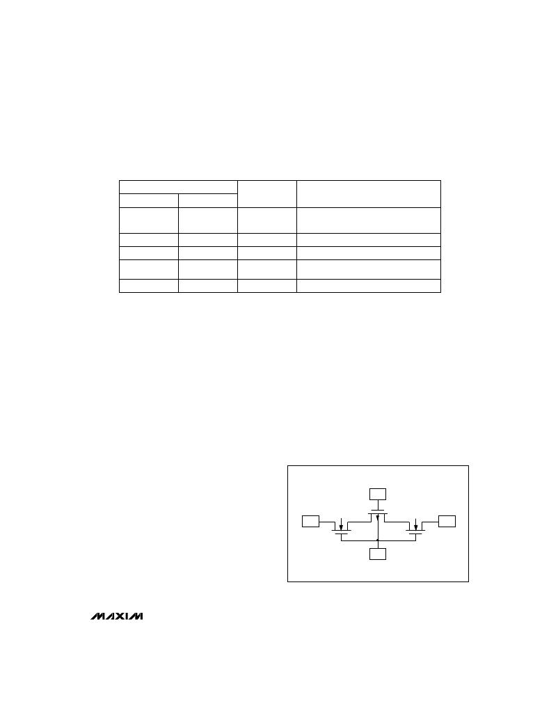
�Internal� Construction�
�Figure� 1� shows� the� simplified� internal� construction� of�
�each� protector� inside� the� MAX366/MAX367.� Each� circuit�
�consists� of� two� N-channel� FETs� and� one� P-channel� FET.�
�All� the� FETs� are� enhancement� types;� that� is,� the� N� chan-�
�nels� must� have� approximately� 1.3V� of� positive� gate� volt-�
�age� in� order� to� conduct,� and� the� P� channel� must� have�
�approximately� 2V� of� negative� gate� voltage� in� order� to�
�conduct.�
�During� normal� operation,� V+� is� connected� to� a� positive�
�potential� and� V-� is� connected� to� a� negative� potential.�
�Since� their� gates� are� tied� to� V+,� transistors� Q1� and� Q3�
�conduct� as� long� as� their� sources� are� at� least� 1.3V� below�
�V+� (the� N-channel� gate� threshold.)� Transistor� Q2’s� gate�
�is� tied� to� V-,� so� it� conducts� as� long� as� its� source� is� 2V� or�
�more� above� V-� (the� P-channel� gate� threshold.)�
�V-�
�P�
�Unlike� shunt� diode� networks,� these� devices� are� low-�
�impedance� FETs� that� become� high� impedance� during� a�
�fault� condition,� so� fault� current� and� power� dissipation� are�
�IN�
�N�
�Q2�
�N�
�OUT�
�extremely� low.� Equally� important,� leakage� current� during�
�normal� and� fault� conditions� is� extremely� low.� In� addition,�
�Q1�
�V+�
�Q3�
�unlike� most� discrete� networks,� these� parts� protect� circuits�
�both� when� power� is� off� and� during� power� transitions.�
�Figure� 1.� Simplified� Internal� Structure�
�_______________________________________________________________________________________�
�5�
�发布紧急采购,3分钟左右您将得到回复。
相关PDF资料
MAX4080EVKIT+
KIT EVAL FOR MAX4080
MAX4208EVKIT+
KIT EVAL FOR MAX4208
MAX4209EVKIT+
KIT EVAL FOR MAX4209
MAX4210EEVKIT
EVAL KIT FOR MAX4210
MAX4273EVKIT
EVAL KIT FOR MAX4273
MAX4278EVKIT-SO
KIT EVALUATION FOR MAX4178,4278
MAX44265EVKIT#
KIT EVAL FOR 44265
MAX4754AEVKIT+
KIT EVAL FOR MAX4754
相关代理商/技术参数
MAX367CWN+
功能描述:隔离器接口集成电路 Signal Line Circuit Protector RoHS:否 制造商:Texas Instruments 通道数量:2 传播延迟时间: 电源电压-最大:5.5 V 电源电压-最小:3 V 电源电流:3.6 mA 功率耗散: 最大工作温度:+ 125 C 安装风格: 封装 / 箱体:SOIC-8 封装:Tube
MAX367CWN+T
功能描述:隔离器接口集成电路 Signal Line Circuit Protector RoHS:否 制造商:Texas Instruments 通道数量:2 传播延迟时间: 电源电压-最大:5.5 V 电源电压-最小:3 V 电源电流:3.6 mA 功率耗散: 最大工作温度:+ 125 C 安装风格: 封装 / 箱体:SOIC-8 封装:Tube
MAX367CWN-T
功能描述:TVS二极管阵列 RoHS:否 制造商:Littelfuse 极性: 通道:4 Channels 击穿电压: 钳位电压:11.5 V 工作电压:2.5 V 峰值浪涌电流:20 A 安装风格:SMD/SMT 端接类型:SMD/SMT 系列: 最小工作温度:- 40 C 最大工作温度:+ 85 C
MAX367EPN
功能描述:热插拔功率分布 RoHS:否 制造商:Texas Instruments 产品:Controllers & Switches 电流限制: 电源电压-最大:7 V 电源电压-最小:- 0.3 V 工作温度范围: 功率耗散: 安装风格:SMD/SMT 封装 / 箱体:MSOP-8 封装:Tube
MAX367EPN+
功能描述:热插拔功率分布 Signal Line Circuit Protector RoHS:否 制造商:Texas Instruments 产品:Controllers & Switches 电流限制: 电源电压-最大:7 V 电源电压-最小:- 0.3 V 工作温度范围: 功率耗散: 安装风格:SMD/SMT 封装 / 箱体:MSOP-8 封装:Tube
MAX367EWN
功能描述:热插拔功率分布 RoHS:否 制造商:Texas Instruments 产品:Controllers & Switches 电流限制: 电源电压-最大:7 V 电源电压-最小:- 0.3 V 工作温度范围: 功率耗散: 安装风格:SMD/SMT 封装 / 箱体:MSOP-8 封装:Tube
MAX367EWN+
功能描述:热插拔功率分布 RoHS:否 制造商:Texas Instruments 产品:Controllers & Switches 电流限制: 电源电压-最大:7 V 电源电压-最小:- 0.3 V 工作温度范围: 功率耗散: 安装风格:SMD/SMT 封装 / 箱体:MSOP-8 封装:Tube
MAX367EWN+T
功能描述:热插拔功率分布 RoHS:否 制造商:Texas Instruments 产品:Controllers & Switches 电流限制: 电源电压-最大:7 V 电源电压-最小:- 0.3 V 工作温度范围: 功率耗散: 安装风格:SMD/SMT 封装 / 箱体:MSOP-8 封装:Tube